The consumer electronics industry primarily uses flat-panel display (FPD) technology based on glass substrates as its core display technology. Various advancements and extensions of the FPD technology, such as LCD, OLED, Micro LED, and QLED, are continually developing. At the substrate level, there is no fundamental difference in the essential unit of the driving backplane, known as the thin film transistor (TFT).
As the consumer electronics industry continues to grow, display makers are increasingly pushing the boundaries of display capabilities through the development and mass production of silicon-based displays. This trend is particularly highlighted by the recent launch of the Apple Vision Pro. Silicon-based displays represent a significant breakthrough in FPD technology, where the fundamental backplane driver component has transitioned from TFT to metal-oxide-semiconductor field effect transistor (MOSFET) in OLEDoS.
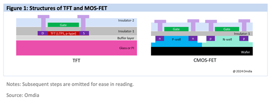
Theoretically, TFT is a type of MOSFET, but TFT is a transistor made on the glass substrate. The MOSFET in this blog specifically refers to the transistor structure based on a wafer substrate. Figure 1 shows their differences.
Current-driving and voltage-driving pixel circuit differences
The pixel circuit designs are divided into voltage-driving and current-driving solutions. Controlling the voltage of components is relatively easy, while controlling the current is more complex. As a result, two main pixel circuit design schemes have been formed, as shown in Figure 2.
In the micro display industry, both OLEDoS and LEDoS initially utilized voltage driving. The demand for current-driving products for OLEDoS is rising, particularly due to the VR and MR trends spurred by Apple Vision Pro. However, because of LEDoS’ long lifespan and the fact that many products are still in early development, voltage driving remains the mainstream approach.
Pixel driving circuit for silicon displays
The pixel circuit of an actively controlled OLEDoS and LEDoS requires at least two transistors and one capacitor in each lighting structure (commonly known as a subpixel). One of the two transistors is used as a valve to control the current through the OLEDoS and LEDoS, generally referred to as a driving transistor. The other transistor is mainly used as a switch to charge the capacitor and is called a switching transistor.
To achieve more complex functions, the switching transistor will be composed of more complex circuits. This will ensure that each driving transistor on the panel operates as required and will enhance the reliability of the driving transistor as much as possible.
Figure 3 shows the schematic diagram of the LEDoS and OLEDoS driving circuits, as shown in two patents.
For detailed insights into the near eye display market, click here for Omdia’s latest report. Further analysis covering display market trends and industry forecasts prepared by Omdia’s Display practice can be found here.
More from author
More insights
Assess the marketplace with our extensive insights collection.
More insightsHear from analysts
When you partner with Omdia, you gain access to our highly rated Ask An Analyst service.
Hear from analystsOmdia Newsroom
Read the latest press releases from Omdia.
Omdia NewsroomSolutions
Leverage unique access to market leading analysts and profit from their deep industry expertise.
Solutions


